SEM Magnification Calibration and Verification: Building Confidence in Your Scale Bar
November 1, 2018
Presenter: Mak A. Koten, Ph.D., Senior Research Scientist, McCrone Associates
Regardless of whether you are an academic researcher or industrial laboratory specialist, all scanning electron microscope (SEM) operators are confronted by their scale bar at some point. The burning question is usually something like, “How do I know this scale bar is accurate?” Mak breaks down this question in detail and explains how the scientists at McCrone Associates ensure that the scale bars in their SEM images are accurate.
Download the slides and the transcript.
Attend an online course in Scanning Electron Microscopy offered by Hooke College of Applied Sciences, a member of The McCrone Group.
![]()
Transcript
Charles Zona (CZ): Hello, and welcome to another McCrone Group webinar. My name is Charles Zona, and today we welcome Mak Koten. Mak is going to talk to us about “SEM Magnification Calibration and Verification: Building Confidence in Your Scale Bar.” Before we get started, I would like to give you a bit of Mak’s background. Mak is part of McCrone Associates’ electron optics group, where he specializes in materials characterization and phase identification via a combination of X-ray diffraction, scanning electron microscopy, energy dispersive X-ray spectroscopy, and transmission electron microscopy. He designs and conducts experiments that will help clients better understand and solve specific problems such as product contamination, product specifications failure, and unknown manufacturing or processing issues. He is also one of the instructors for our Scanning Electron Microscopy course here at Hooke College of Applied Sciences. Mak will field questions from the audience immediately following today’s presentation. This webinar is being recorded and will be available on The McCrone Group website under the Webinars tab. Now, I will hand the program over to Mak.
Mak Koten (MK): Thanks, Chuck, for that warm introduction, and thank you all for joining us this afternoon for our webinar! We are very pleased to have you. The topic I would like to discuss today is one of great importance to an SEM operator, and that is how to ensure that measurements made from SEM images are accurate. In any project I’ve done where measurements are made, this question always gets asked by the client, and it is an important question, so we wanted to address it in some detail here today.
When you ask yourself if the measurements you are making are accurate or not, what you are really asking yourself is, “Has this SEM been properly calibrated?” Some labs have protocols in place where this is checked at regular intervals. Here at MA, for example, we check this annually, or after a major service call.
You may think that the SEM service engineer has calibrated the instrument so you don’t have to worry about it, but they don’t always use traceable standards for that calibration.
Who usually checks the magnification calibration? In academia, it is usually the microscope specialist or lab manager, or an experienced user that is concerned about calibration. In an industrial lab, there may be a particular operator appointed to checking the calibrations.
It may also be required for accredited laboratories, such as if you have an ISO 17025 accreditation.
So to begin this discussion, I will introduce some of the relevant concepts concerning calibration and verification, and I will begin with the concept of magnification.
SEM magnification is defined as the ratio of a length measured from the SEM monitor—Lm—to the same length measured on the sample—Ls. M equals Lm over Ls. The length measured can be anything from the side of a single pixel all the way up to the entire horizontal or vertical field of view. The ratio of each length should be the same, that is, they should yield the same magnification.

If we look at this equation, we see that the monitor length is fixed, so if the magnification, M, is to change, that means that the value of Ls must change. The SEM takes care of this by changing the distance the beam is moved over the sample. Shorter distances result in higher magnification images.
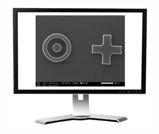
In almost all SEM images, you will see a data bar somewhere in the image, like the one shown here. It’s usually somewhere at the bottom. Something it nearly always includes is a nominal magnification. I say nominal because it only applies to images that are viewed on the microscope PC. The one shown here has a value of 35,000X, but it would not be accurate if the same image is viewed on any other screen.
In these three examples, Lm1 is supposed to represent the original image being viewed on the microscope PC. So, this is the microscope PC. Lm2, then, is the same image being viewed on a laptop computer, and Lm3 would be yet a third length obtained by the image that is projected onto a projection screen, say, if you were giving a PowerPoint presentation.
For these three copies of the same image, we have one value of Ls, corresponding to the actual horizontal field of view of the image, for example, in microns. But we see that Lm is always changing unless we measure from the microscope PC. Therefore, the actual magnifications are different in these three cases. I’m calling this the magnification paradox because as soon as the image is opened up on a different computer than the microscope PC, the magnification burned onto the image is wrong.
Now I will give some examples of magnification calculations, except here, I’m going to actually calculate the value of Ls that would be obtained from a specific magnification.
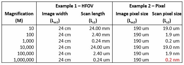
The first column in this table shows the magnification range typical for an SEM: about 10X to 1,000,000X. In example one, I’m using the horizontal field of view of the image, that is, the entire width of the image, for my value of Ls and Lm. So you can see in the second column that the values for Lm1 stay constant—24 cm is what we measured on our microscope PC. However, the values for Ls1 scale according to the magnification. This illustrates how the field of view is changed in an SEM just by lengthening or shortening the raster distance.
Similarly, in example two, I have the width of a single pixel in the image as my length in the calculation. By dividing the value for Lm in example one by the number of pixels in the image 1280, we see that each pixel is being displayed on the microscope PC as being 190 microns a side, which stays constant. At each magnification, the value of Ls2 then is calculated and we can see how short the pixel-to-pixel raster distance must be for the SEM to achieve this magnification. At 1,000,000X, the distance between two pixels is on the order of .2 nanometers.
A side note about vertical field of view is that this data bar at the bottom can sometimes change this value. In our example, we had in the SEM microscope settings, the value listed for the image resolution was 1280 x 960 pixels, but this data bar actually adds another 64 pixels to the image, so it changes the overall image resolution to be 1024 x 1280. The reason this matters is, if you try to repeat example two on your microscope for the vertical field of view instead of the horizontal, then you would have to select the corresponding image resolution to either include or exclude the data bar.
Next, I’m going to talk about SEM image formation. If you are an SEM user, you probably know that the SEM is not like other microscopes. Namely, that the process by which images are formed is different. You cannot draw a ray diagram for the SEM, for example, like you can with an optical microscope, or a TEM.
This is because an image is not projected onto a camera after passing through the optical system, but rather the beam of electrons is being precisely controlled by a scan generator, which deflects the beam over the sample in a grid pattern.
The detector collects electrons—both secondary and backscattered electrons—for each beam position in x and y space and saves the number of electrons detected at each beam position. The example below shows the intensity plot for a single line in the image.
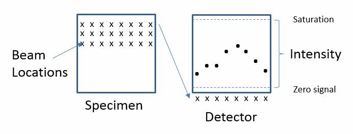
Finally, the computer is able to map this information onto a file with a readable format that can display the electron intensity measured at each beam position on the computer screen as a digital image.
It is here that we arrive at the crux of the calibration discussion for an SEM. What is actually being calibrated in the SEM is the distance the beam moves in both the x and y directions. Both the precision and the accuracy of the scan generator are important for image quality and measurement.
Because the beam positions will be mapped to a square grid in the image—that is to say the square, periodic pixels that make up an image—the actual motion of the beam must be square. If this is not the case, distortions in the image will arise. Similarly, if the distances between the beam positions are not accurately known, then measurements made from the images will be poor.
In the diagrams below, the one on the left shows a certain kind of distortion. The pixels are stretched in the horizontal direction. This will cause the object in the image to appear horizontally compressed. The example on the right is the opposite effect, and it will result in vertical compression.
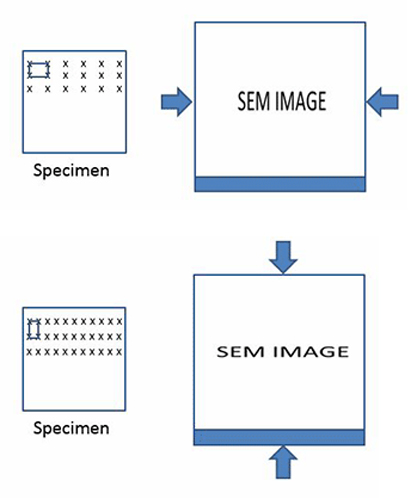
BOTTOM: Vertical compression.
Distortions such as these are a nightmare for an electron microscopist, because they are very hard to see when viewing your samples. Later on, I will show you the type of sample you can use to evaluate your scan generator in terms of the image distortions.
At this point, I have introduced the digital resolution in the form of pixel size, and its relationship to the scan generator, but what else goes into forming an SEM image? The image resolution is not always the same as your digital resolution. This is particularly true at higher magnifications.
Such factors as probe size, interaction volume, and even the realistic shape of the beam play important roles in the actual image resolution.
The diagram on the right shows the idealized picture of a focused beam of electrons scanning across a sample. The grid below is meant to represent the beam positions that make up the pixels in the final image. The beam is placed at each position, but these other factors can sometimes cause considerable overlap from position to position.
Interaction volume depends on voltage and increases with beam energy. The beam is not perfectly collimated, but rather it has a Gaussian shape, meaning some electrons land on your sample outside of the expected probe size, which is often quoted as the full width half max (FWHM) of the Gaussian profile.
The updated diagram shows the Gaussian profile extending outside a single pixel into neighboring pixels. Spurious signal can be detected outside of the confined region of each position.
We have already calculated the range of pixel sizes for typical SEM images, and it is interesting to note that—especially for thermionic sources—the probe size can be significantly larger than the pixel size. This reduces your image resolution compared to the digital resolution, particularly at higher magnifications.
Next, I would like to some of the advantages you do save an image with a scale bar get when value of the scale bar, versus when you don’t save the image with a scale bar.
If you only have the nominal magnification, then you don’t have any value of Ls from the magnification equation from before to help you in making measurements from the image, or in recalculating the magnification, if you are interested in doing that. You can always calculate—or measure—the value of Lm, from the screen that you’re using, but the saved magnification is no longer valid, so features in your image can’t be measured at a later date on a different PC, and if you want to measure something you have to go back to the microscope PC, which you might not always have access to, so it’s inconvenient.
If you have the scale bar, then you always have a measurement of Ls that’s embedded in the image and travels with the image—saved in the image, so any number of calculations and measurements can be made using that.
You can always measure the value of Lm if you wish to calculate the new magnification of your image, and you can make measurements of sample features at a later date on any PC, as long as you have the software that can open up your image. And something that’s undervalued, I think, is that another person can much more easily look at your image and see what the size of the features are. So, in the example on the right, here I have two images, and they’re the same image, but one has a scale bar and one doesn’t. In the top image, if you just glance at it, you can see that the magnification is 1600X, but that doesn’t really give you a good idea of how large that window is. Whereas, in the image below, you can see the 10 µm scale bar, and that does give you a much better, clearer, indication of how large the features are in the image.
We say that including the scale bar is a good practice, and excluding it is not a good practice.
Like I mentioned on the last slide, one of the biggest advantages of having the scale bar saved on the image is that it allows you to import a pixel-to-length unit conversion factor into most image analysis software for advanced analysis techniques.
Advanced image analysis is often done in third party software such as ImageJ or Image-Pro, which can be used to make complete, complex measurements of samples. These include thresholding for particle sizing or segmentation, and can extend to development of procedures that are automated and can be run on image stacks or a batch of files.
These measurements often require the software to know the length of your scale bar in both pixels and real length dimensions. From your scale bar you can obtain a pix/nm or µm conversion factor. Just measure the length of your scale bar in pixels and divide that by the length in real units. There is usually a set scale function that allows for the software to apply this ratio to the image or image stack.
In this image, you can see the software knows the image resolution in pixels, which is 1280 x 1024. The software has arbitrarily assigned a real dimension of inches to the image. This is what I want to see change. So I will measure my scale bar, which has a known distance of 500 nm, and I will import the length in both pixels and nm, leave the aspect ratio at 1.0, and ImageJ computes the conversion factor, down here, at 0.35 pix/nm. Then it changes the dimensions on the image so they’re in nm.
So what we did is we used the native resolution in pixels, and a conversion ratio to obtain the actual distance swept out by the electron beam in nm.
Now I will discuss the type of sample and specific sample features that make for a good image calibration tool.
The first thing we need is for the sample to be made of something that is both chemically and structurally very stable at ambient conditions. We also want the sample to have sharp edges or transitions between features of known sizes, at the highest possible magnifications. Since SEMs can reach up to 1,000,000X, this is not a small request.
For calibrating lengths, something periodic is ideal, but because of the large mag range in an SEM, we need this periodic structure to be recognizable at very high and very low magnifications. This means it would have to span about four orders of magnitude, and the pitch has to be very accurate and constant over that entire range—also not a simple request!
The image to the right is ideal for calibrating images, whereas the images below are not. TEM grids are not suitable because they are only to be viewed at lower magnifications. The smallest feature fills the screen at 3000X. Their edges are not very sharp either, which makes it hard to measure distances accurately. Another bad example is using a human hair! Even if you do know the width of the hair accurately, it is not small enough for higher magnifications.
The best sources for calibration verification are known as Standard Reference Materials, or SRMs, and they come from National Metrology Institutes all over the world.
A National Metrology Institute (NMI) is a national laboratory that is tasked with the realization, maintenance, improvement, and dissemination of the SI units via traceable calibration and measurement services based on their calibration and measurement capabilities.
In the US, our NMI is NIST; the National Institute of Standards and Technology. The NIST website lists all of the NMI labs for each country. Some of the others include the UK’s NPL, National Physical Laboratory; France’s LNE, and Germany’s PTB. I won’t try to pronounce the actual names of the last two.
The key to making an SRM is traceability.
You want to choose an SRM that is traceable back to an NMI like NIST. This means that an unbroken chain of validation from processing to measurement exists for the material. Sample to sample uncertainties are known an acceptable, which accounts for errors in manufacturing. Measurement uncertainties are known and acceptable. These are the requirements to satisfy Category I traceability for an ISO 17025 accreditation body.
Some good examples are the MetroChip, which is made by MetroBoost. This is what we currently use for our SEM calibration and verification. NIST has RM 8820, which is a similar artifact for calibration to the MetroChip. Another option for SEM mag calibration is the MRS-6 reference standard that is also made by NIST. Finally, for TEM image and diffraction calibration, a great sample is the MAG*I*CAL x-section. The MAG*I*CAL calibration sample is directly traceable to the lattice constant of silicon <1 1 1> (0.3135428nm). This constant can be measured directly on the MAG*I*CAL sample, providing unbroken traceability to a fundamental physical constant in nature.
All of these are available from Ted Pella, except for the RM 8820 which is sold by NIST.
As I mentioned on the last slide, our current SRM of choice is the MetroChip. To understand the traceability of this reference standard, one has to begin with the microfabrication process that is used to manufacture it. It is manufactured using a type of advanced semiconductor processing known as photolithography.
In this method a thin-film heterostructure is grown on a pure single crystal silicon wafer. On top of that is a native oxide layer that is about 5 nm thick, and deposited on top of that is a polycrystalline Si film 150 nm thick. This is then coated with a photoresist and then covered by a photomask. The top surface is exposed to light, which develops the resist in unmasked regions. The developed resist is selectively washed away, leaving the undeveloped resist and exposed polysilicon film. The wafer is then exposed to a plasma, which sputters away the polysilicon in the exposed region until it reaches the oxide (SiO2) layer. The undeveloped photoresist is then cleaned off of the surface leaving an etched surface that mirrors the original mask.
This microfabrication technique is optimized to yield very accurate periodicity at the expense of variations is feature sizes. The kind of periodic structures found in this sample are illustrated here. There is a periodic pattern of lines and spaces; together they add up to what is called the pitch for that sample. This is important to know, since pitch is the distance that should be measured and not the line or space width.
The green and blue patterns shown here clearly have different linewidths, but when they are overlapped, we see that they have the same pitch. MetroBoost guarantees pitch rather than linewidth, which is why it is important to know the difference and measure the right one.
Finally, this image shows measurements of line and space width rather than pitch. These are not the right way to measure for image calibration.
So you might be wondering how NIST certified the MetroChip. They first determined the reliability of pitch from sample to sample, showing that the deviation is very low, on the order of 2 ppm. So the reliability is very high for pitch.
Next NIST used their line scale interferometer to certify the accuracy of the pitch on a single MetroChip surface. This was done by overlapping an interference pattern and counting the fringes on the actual surface of the MetroChip.
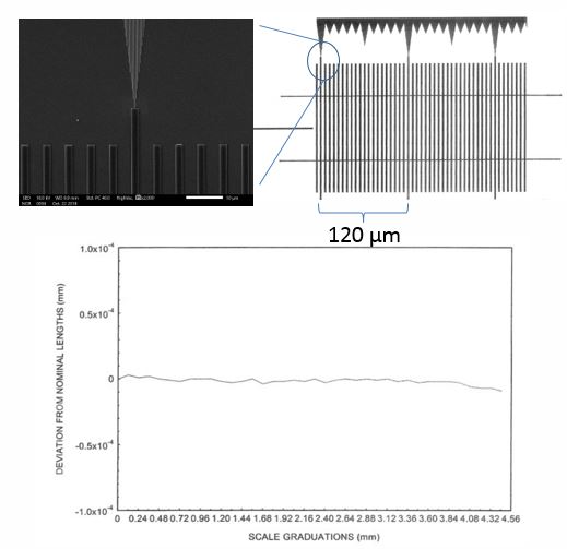
This means that the pitch for all metro chips is both accurate and reliable if made from the same mask NIST certified. MetroBoost only uses that mask for fabrication of metrochips. This does not mean that other features within the pitch of the microrulers are validated. They are not. For example, height, linewidth and sidewall angle were not certified by NIST. These features can vary up to +/–10 percent.
So now that we know what to use for the calibration procedure, how do we calibrate our microscope? The short answer is, in most cases we don’t, but a vendor service engineer might.
Most SEM vendors perform annual preventative maintenance activities. You want to take advantage of these visits to make sure that your SEM magnification is properly calibrated.
How do the vendors actually change the calibration? They have to change the pixel-to-pixel raster distance. Older SEMs have scan generators that can be adjusted via potentiometers by the service engineer. Newer SEMs are corrected digitally during the mapping process within the SEM operation software.
Some vendors will perform calibrations with traceable SRMs to a recognized authority, but others will not. You may be able to ask them to use yours if they aren’t using one.
It’s a good idea to perform your verification while the service engineer is still on site, since you will need their help if the verification fails.
So the best we can do is check that the microscope has been properly calibrated by the vendor. How do we do that?
Well, our general procedure is to:
- First, set up your instrument for SEM imaging with the MetroChip installed, then
- Locate the calibration rulings on the MetroChip for both x and y orientations
- Capture images of both the x- and y-oriented rulings without rotating your scan or stage
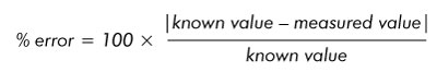
- Calculate the percent error with this formula:
- Make sure the distances measured in both x and y directions meet your acceptance criteria (5% is what we use here at MA). This will verify that both x and y are accurate and not distorted, which is important for reasons I mentioned earlier during the discussion of image formation.
In the example shown here, I have taken four measurements, each with a different number of periods. This was done on the smallest ruler on the MetroChip, which has a pitch of 250 nm. I calculated the percent error for the four measurements, and you can see that as the periods increase, the percent error decreases. This is something to keep in mind at very high magnifications. Best practices dictate that you take the longest measurement you can in the image.
Also note that the magnification here is 100,000X. So that is much better verification than measuring a hair or TEM grid at 1000X.
Here are some other features available on the MetroChip that are useful for SEM image validation.
We have mainly been talking about the linear microscales, of which there are two on the MetroChip that were NIST certified. They are orthogonal to one another so that you can measure both the x and y directions separately. The smallest pitch available on the MetroChip is 250 nm, but they also offer 300 and 400 nm. Some other reference standards go as low as 80 nm in pitch, which allows you to reliably test even higher magnifications, but it will cost you. These are more pricey.
Scatteronomy targets are also available for use on the MetroChip. These can also be used for magnification calibration, however, these features were not tested directly by NIST.
Finally, there are many distortion targets that can be used for calibrating a wide range of fields of view. These can come in handy if you are concerned about your image being squeezed or stretched in the x or y direction.
It is also important to keep your reference standard clean, but if you are using a device made from advanced microfabrication techniques, then you’ll want to know what to do and what not to do to clean it. Let’s start with the what not to dos.
Things to avoid include:
- Wiping the sample with a cloth. This will destroy the features.
- Spraying the sample with gases that leave residue.
- Immersing the sample in liquids that leave residue.
- Using cleaning solutions that attack silicon dioxide.
- Avoid plasma treatments that attack silicon dioxide. These include gas mixtures containing chlorinated gases.
- You also want to avoid harsher plasma treatments, such as those using chlorinated gases. These will etch the silicon layer.
Good cleaning procedures include:
- For large particle removal, nitrogen gases and sprays can be used, such as Dust-off.
- You can also rinse the sample in DI water.
- For cleaning fingerprints, chemical baths that remove photoresist, if available, are effective.
- Plasma sample cleaners with pure oxygen, or forming gas can be used safely for removing fingerprints and hydrocarbon residues.
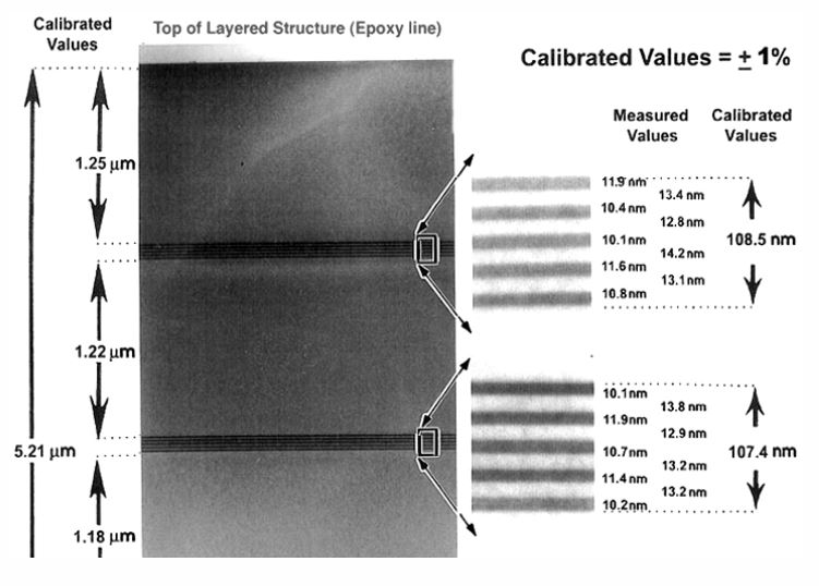
Finally, I will briefly describe the MAG*I*CAL reference standard for TEM magnification calibration. One of the challenges in calibrating TEM images is in finding a sample you can use for the entire mag range. The MAG*I*CAL sample was designed specifically for this purpose.
It is a cross-sectional TEM sample with alternating layers of silicon, germanium alloy, and silicon. It was grown via molecular beam epitaxy (MBE) on the <111> direction of a single crystal silicon wafer. Four sets of five alternating layers make for a wide range of image magnifications. Top to bottom this feature is 5.21 µm long, and it is broken up into 1.2 µm sections. Then, the silicon-germanium layers are about 10 nm thin—overall, 100 nm. So you are getting some of the idea of the range designed into this sample.
Additionally, since the heterostructure is epitaxial, phase contrast imaging can also be used for high resolution TEM calibration at the highest magnifications, and in diffraction mode you can also use it for camera length calibration.
To conclude this webinar, I would like to highlight some of the important points made throughout the presentation.
- SEM image formation depends on the accuracy and precision with which the scanning device moves the beam over the sample.
- Remember: you cannot draw a ray diagram for the SEM.
- The pixel-to-pixel raster distance is responsible for changing the magnification in an SEM, and if that distance is accurately known, it is also responsible for image calibration. We are trying to make sure there is a 1:1 correlation between the distance between adjacent beam positions and adjacent pixels in the image.
- To properly calibrate an SEM, a traceable standard reference material must be used. We have listed a few examples here including the MetroChip and MRS-6 SRMs.This means a NMI has evaluated the production line used in manufacturing the SRM and has deemed the measurement uncertainties acceptable for the measurement in question.
These aspects of SEM image calibration and verification have been discussed in detail here for the MetroChip SRM, which is what we use here at McCrone Associates for our quality assurance program.
That concludes the webinar presentation. Thank you for joining us this afternoon. We hope that this discussion highlighting the traceability of the MetroChip has successfully illustrated the details that go into selecting and using an SRM for magnification calibration and verification.
CZ: Okay. Interesting stuff, there, Mak. Thanks for a great webinar. Thanks to everybody for attending today’s webinar. If you have any questions, please go ahead and type them into the questions field. And while you were giving your webinar, we did receive a question from Bill: “How much does the MetroChip cost?”
MK: That’s a good question, Bill. All of the reference standards that I mentioned are available through Ted Pella, which is one of the leading vendors in electron microscopy accessories and supplies. The MetroChip is one of the more moderately-price reference standards, and it costs about $750.
CZ: Alright. We have a question from Christine: “Are the scale bars accurately sized to the value listed in the image?”
MK: That’s another good question. The short answer is yes. However, there are two types of scale bar. The first is one that most vendors currently use, which is where they adjust the scale bar length to a whole number with a reasonable length for the space provided. Other SEM vendors will give a fixed scale bar length in pixels and just compute the length at the magnification used. Both are equally accurate, and it is an easy thing to test. Just make a few linear measurements using the microscope software and save them in the image. Then open the image up in a third-party program and set the image scale using the scale bar. You can then trace your linear measurements from before and re-measure them to see how measurements derived from your scale bar compare to measurements made directly in the microscope software. They should agree to within less than one percent error.
CZ: Okay, this question is from Jane: “Does the MetroChip need to be coated to view without charging?”
MK: Actually, no, it doesn’t need to be coated, because it’s made from a silicon wafer, which is a semiconducting material, which does not charge in the SEM. Its features are also visible optically and can be used to calibrate optical microscopes, so coating it may interfere with this capability. You don’t have to coat it, but it’s a good idea to keep it clean, as was previously discussed.
CZ: Okay, Mak. Thanks. Thanks, everyone, for the questions, I think that will do it for the questions. If any others roll in, Mak will be happy to answer those offline.
Be sure to check out our list of upcoming webinars that will be posted shortly, under the Webinars tab on The McCrone Group website for 2019, and we hope to see you then. Thanks.
Comments
add comment