The New NeoScope
July 11, 2016
Presenter: Jeff McGinn, President and COO, McCrone Microscopes & Accessories and Hooke College of Applied Sciences
Editor’s Note: This webinar aired in 2016; there is a newer model of this benchtop SEM available.
Benchtop scanning electron microscopes (SEMs) have come a long way since they were introduced. With capabilities including magnifications up to 60,000X, multiple accelerating voltages, and both SE and BSE detectors, these smaller versions of full-size SEMs are increasingly finding their way into industrial and educational laboratories. Whether used by trained electron microscopists as a simple screening instrument, or by lab technicians as a higher-resolution alternative to the light microscope, these powerful instruments accelerate the pace of research in the life sciences, forensics, and pharmaceutical fields. Learn about the new JEOL NeoScope JCM6000Plus offered by McCrone Microscopes & Accessories. 20 minutes.
Transcript
Charles Zona (CZ): Hello and welcome. My name is Charles Zona and I would like to thank everyone for attending today’s McCrone Group webinar.
Our presenter today is Jeff McGinn. Jeff is going to tell us about JEOL’s new scanning electron microscope, the NeoScope. But before we get started, I’ll give you a bit of Jeff’s professional background. Jeff is the president and chief operations officer of both McCrone Microscopes & Accessories (MMA) and Hooke College of Applied Sciences. He teaches portions of Hooke College’s Polarized Light Microscopy courses and has a keen interest in chemical microscopy. He is also well versed in scanning electron microscopy and helps to solve customer’s analytical needs on a daily basis.
Jeff will field questions from the audience immediately following today’s presentation.
This webinar is being recorded and will be available on The McCrone Group website under the “Webinars” tab. And now I will hand the program over to Jeff.
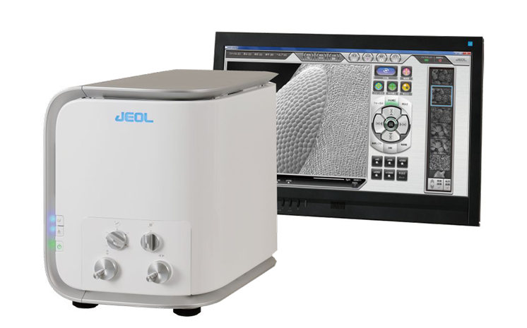
Jeff McGinn (JM): Thanks Chuck and good afternoon everyone. Again, my name is Jeff McGinn and today I’m going to talk to you about the new JEOL JCM-6000PLUS benchtop SEM.
This is the third generation of this exciting instrument, and over the next 10-15 minutes I will discuss some of the key features of this microscope.
Benchtop scanning electron microscopes (SEM) have come a long way in the years since they were first introduced. With capabilities including magnifications up to 60,000X, multiple accelerating voltages, and both secondary and back-scattered electron detectors, these smaller versions of full-size SEMs are finding their way into more and more industrial and educational laboratories.
Here we have some of the key features of the JCM-6000PLUS starting with—
- The overall size—a very small footprint that fits onto any common laboratory bench and plugs into a standard outlet. You do not need to build out a room or reinforce a floor for these types of instruments.
- It has a combined tungsten filament and cartridge-type Wehnelt
- It has real magnification up to 60,000X. I highlight REAL magnification because other benchtop SEMs on the market only go to the 30,000X range then higher with digital zoom.
- The resolution is around 15 nanometers on this instrument.
- It has both high and low vacuum modes for a variety of conductive and non-conductive samples.
- Two imaging detectors, both a secondary and a back-scattered.
- It is the only benchtop on the market with 3 accelerating voltages, 5, 10, 15 kV.
- It has a tilt/rotate motorized sample holder. It has a large chamber that can accommodate samples up to 70mm in diameter and 50mm high. It tilts 15° in one direction and 45° in the other, and has a full 360° rotation.
- And there are a couple of options for the OS, a fully motorized X-Y stage and an EDS detector, which I will talk about more later.
The JCM-6000PLUS has been designed to cover a wide range of applications—these next three slides focus on some of our more common applications such as semiconductor and polymer research.
On this slide, we see two images taken of the same field of view; one under secondary imaging and the under back-scattered.
Here is another image of a semiconductor sample taken under secondary and back-scattered imaging. Note the differences in contrast, particularly on the back-scattered image, noting the changes in elemental composition.

Here we have nice representation of some of the higher-end magnification and resolution capabilities that the NeoScope can achieve. We have two images here of polymer nano fibers, both under secondary electron imaging. The one on the left is at 10,000X, and the one on the right at 20,000X.
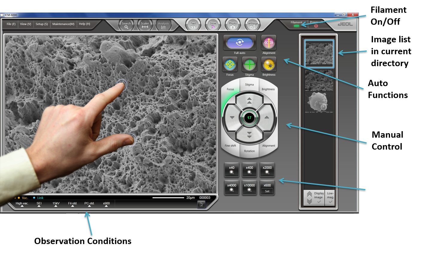
Workflow on this instrument is key, and JEOL has designed a software and overall functionality geared towards ease-of-use. A sample can be loaded, chamber evacuated and image displayed in less than three minutes.
Instrument control via the software can either be done the automatic mode or manually, if desired. As I mentioned previously, we have placed these instruments in full-on research labs with experienced scanning electron microscopists, as well as quality control labs, and with users with little or no SEM experience. We can fully train and get someone up and running in less than an hour.
Once again, software control is simple on the JCM-6000PLUS. This intuitive system features automatic and manual controls, all to control beam alignment, focus, stigmation, brightness, and contrast.
It has an auto filament on/off functionality in order to preserve filament life, as well as preset magnifications. Observation conditions are also fully controllable, including probe current, accelerating voltage and high or low vacuum capabilities.
The system comes standard with touchscreen functionality—perfect for a modern-day generation used to using iPads and iPhones.
Maintenance on the JCM-6000PLUS is as simple as changing a light bulb. Cleaning and centering are not required and axis alignment is automatic. The tungsten filament on this instrument can be changed in less than five minutes.
Overall, today’s benchtop SEMs contain many of the same features as their larger, full-sized cousins. With multiple accelerating voltages and both secondary electrons (SE) and back-scattered electrons (BSE detectors, these compact instruments provide the user with more flexibility, at a lower cost.
The types of signals produced by the JEOL JCM-6000PLUS include both SE and BSE.
Secondary electrons are inherently low in energy and come from the top few nanometers of the sample surface.
Secondary electron imaging can produce high-resolution images of the sample surface. Topography dominates.
Since the intensity of the BSE signal is closely related to the atomic number of the sample, BSE imaging is particularly useful in providing information about the distribution of different elements within the sample. Brighter areas are indicative of denser, higher atomic number materials. The all-new NeoScope now offers both an Everhart Thornley type SE detector, as well as an improved high sensitivity solid state BSE detector.
This improved solid-state multi-segment backscatter electron detector features three imaging modes—composition, topographic, and shadow, which is a combination of composition and topographic.
Here we see an image of a lead tin solder and the unique differences between a secondary image on the left—note the topographic information, and the backscatter image on the right with the notable differences in elemental composition.
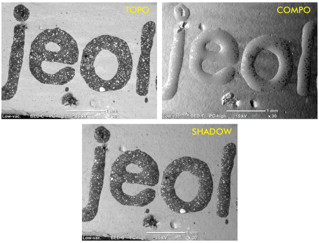
One of the most exciting features of the new JCM-6000PLUS is the improved solid-state multi-segment backscatter electron detector. It features three imaging modes—composition, topographic, and shadow. Shadow is a combination of composition and topographic information.
Here we see three images of the same field of view of a business card—note the differences in elemental composition on the “compo” image, surface enhancement on the “topo” image, and combination of both in the shadow feature.
Measurements are also very easy to perform with the JCM-6000PLUS. One can make direct measurements on the live image itself via the touchscreen or on saved images. Measurements are exported as CSV files.
The JCM-6000PLUS also allows for the ability to compare a live image with a saved one. Here we see a saved image on the right, taken with a stereo microscope, imported into the Neoscope software, and compared with the same field of view in the SEM.
This can also be done in a quality control setting as live images are compared with reference standards that have been captured previously.
New to the JCM-6000PLUS is a motorized x-y control stage. Here on the larger image we see the view position of the stub on the software pop-up window. When we couple this motorized stage with the standard tilt-rotate stage, which we see here on the upper right, we can achieve 4 axis motor control, X, Y, tilt, and rotate.
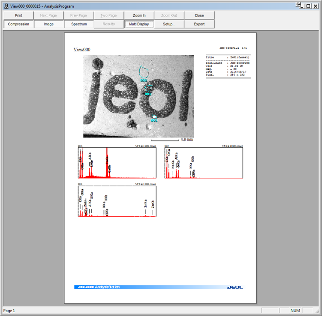
Perhaps the most powerful advancement in the JCM-6000PLUS is the full-featured energy-dispersive X-ray spectroscopy detector or (EDS). This analytical technique is used for the elemental analysis or chemical characterization of a sample. The EDS process detects x-rays emitted from the sample during bombardment by an electron beam to characterize the elemental composition. Features as small as 1 um or less can be analyzed.
And some of the key features on the JCM-6000PLUS EDS are 10mm² silicon drift detector, guaranteed resolution of 133eV or better. It has an ultra-thin window for detection from Boron to Uranium, and offers full area, partial area, multiple point, and line scan EDS analysis. It can acquire up to 32 elemental maps simultaneously, at 4096 x 3072 pixels, and offers drift compensation.
Equipping the JCM-6000PLUS with this powerful technique enables scientists the ability to fully characterize their samples and to identify unknowns, at a fraction of the cost of a full size SEM.
Here we see an X-ray map with detected elements highlighted on the pop-up periodic table. Again, one can perform detection on a spot, area, line, and with x-ray mapping functionality.
The powerful EDS software allows for report generation and places images, spectral, and experimental conditions on to a Word, Excel or PowerPoint document.
One of the many exciting things about The McCrone Group is that in addition to our analytical services and instrument sales, we also offer, through Hooke College of Applied Sciences, training courses in a variety of microscopy techniques. When MMA provides a JCM-6000PLUS to a customer we always include expert installation and instruction, but we also offer Hooke College‘s five-day intensive SEM course.
This five-day course is hands-on and covers things like SEM setup and operation, EDS qualitative and quantitative analysis, and imaging techniques. We encourage you to bring your own samples for use on one of our many SEMs here at McCrone. The JCM-6000PLUS is also used in the course.
And with that, we have come to the end of my presentation. Thank you for your time today.
And, Chuck, I think we are going to take a few questions.
CZ: We have some questions rolling in here right now. From James, “Can you compare the JCM-6000PLUS with a full-sized SEM to help him understand where limitations might be between the JEOL instruments?”
JM: Thanks, Chuck and thanks, James. The full-sized SEM has a higher magnification range, some of them go up to 1,000,000X, a 1,000,000X mag. The NeoScope, JCM-6000PLUS, only goes up to 60,000X. It has three set voltages of 5, 10, and 15 kV, where on a full-sized you might get a much wider range. I hope that helps.
CZ: That’s a good question. From Andy, “What does the full-sized SEM have that the JEOL NeoScope does not?” So, kind of along the same lines.
JM: It’s really the magnification capabilities. Resolution as well, obviously. As I mentioned, the resolution on the NeoScope is near 15 nanometers, and you can certainly achieve much higher, I don’t want to say better, but much higher on a full-sized SEM.
CZ: Andy also followed up with the accelerating voltages that are available.
JM: On the NeoScope, they are 5, 10, and 15 kV, with high and low vac.
CZ: From Jan, “Are the XY coordinates of a particle on a filter stored, so I can make several pictures and stitch them together?”
JM: I would have to get back on that question, Jan. The motorized stage, that is a new item. And you can’t store the coordinates on a basic stage, but I think you might be able to do it on the new one. So, let me check on that and I will get back to you. I think it’s possible, but I am not positive.
CZ: From Stephen, “Were the business cards images coated or they were taken using variable pressure SEM?”
JM: They were coated with a fine layer of gold.
CZ: From Kirk, “Would you say that obtaining a SEM would benefit the biology, chemistry and physics departments at any university?”
JM: Yes, certainly. And, I think Chuck can probably talk about that, too. Many of our students here, they are students at local colleges, and they use SEMs. We have seen a lot of schools that don’t have SEMs and this is certainly a cheaper way to utilize this exciting science.
CZ: Yes, they get it kind of on campus, so to speak. We have had physicists, physics professors, biology professors, and chemistry professors attending our SEM courses. I think they would find a wide application.
From James, “Is the motorized stage and x-ray standard now?”
JM: Well, they can be. You can purchase a benchtop SEM, the NeoScope, with or without those items. So, they are listed, as basically an option, but, yes. You can get it with both.
CZ: From Brian, “Do you think this product is a necessity for a pharmaceutical company in the identification of their particulates?”
JM: Yeah, that would be a definite “yes.” I would say that 75% of our customers are pharmaceutical scientists. It is a benchtop instrument. It is quick and it is easy. As I mentioned before, you don’t have to build out a special room and you can move it from lab to lab, as well.
CZ: From Kirk again, “Is the five-day course only available with the purchase of the SEM system?”
JM: No, it is not. You can take the five-day course without the purchase. Chuck, when is our next course scheduled?
JM: October 24-28, I think.
CZ: Yes. It is a very popular course. We do limit the number of seats as to give people the most hands-on instrument time possible. We try to keep the class small. But, yes. It is available to anyone out there who is interested in learning about scanning electron microscopy.
We have one more question, here. From Andy, “What are the recommended conditions, like humidity, temperature, and vibration?” Shaking he mentions.
JM: There are really no recommended environmental conditions. We place our instrument on a standard lab bench. We have traveled with these before. We put them in the back of our car and traveled with them. Not that we use them there. It needs to be in a standard lab, that’s all. You don’t need to monitor temperature or anything like that. And if it is on a sturdy table, vibration is never an issue.
CZ: I think that is going to do it for the questions. I would like to thank everyone for attending today’s webinar.
Comments
add comment