Transmission Electron Microscopy
The capabilities of the Transmission Electron Microscope (TEM) are applicable to a wide variety of materials, including, but not limited to, nanomaterials, polymers/composites, minerals, glass delamination, pharmaceuticals, and metals and ceramics. In the TEM, a beam of high-energy electrons is transmitted through a thin (<100 nm) sample. Interaction of the primary beam electrons with electrons in the sample atoms produce a variety of x-ray and electron signals that can be collected as images, diffraction patterns and energy spectra.’
The TEM is unique in its ability to provide information about size, morphology, composition, crystallinity and electronic state of a sample, all with extremely high spatial resolution. Because a thin specimen is required, specialized sample preparation techniques such as ultramicrotomy, ion milling or electropolishing are sometimes required. Powders, small particles and colloidal suspensions can often be dispersed on TEM grids with minimal preparation.
Current capabilities include:
- A 3 nm probe for high spatial resolution analysis in all modes of operation
- Imaging lattice resolution of 0.14 nm
- Magnification range of 4 KX to 1.2 MX
- Digital acquisition and processing of images and diffraction patterns; imaging modes include bright field, dark field, backscattered and Z-contrast
- Energy dispersive x-ray spectrometry (EDS) for elemental analysis of boron and higher atomic number elements
- High resolution lattice imaging and electron diffraction to acquire crystallographic structure information
- Electron energy loss spectroscopy (EELS) and energy filtering (EFTEM) to provide electronic state and bonding information
- Ability to operate in scanning transmission mode to acquire EDS elemental maps and linescans, and chemically sensitive maps using energy filtering
- Cold stage for examination of thermally sensitive materials
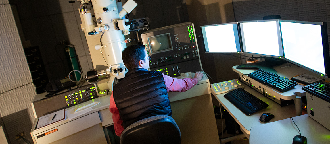
Instrumentation
McCrone Associates uses a JEOL 3010 TEM with:
- 300 kV accelerating voltage with a LaB6 electron source
- High-tilt/high-resolution pole piece
- STEM and backscatter detectors
- Gatan 1.3k x 1k anti-blooming CCD camera for digital acquisition of diffraction patterns
- 2k x 2k high-resolution imaging CCD camera
- Electron energy loss spectrometer and imaging filter with spectrum imaging
- FasTEM software for integration of all microscope operations
- Digital Micrograph software for CCD camera control and digital image analysis
- Oxford INCA energy dispersive x-ray spectrometry system with 80 mm2 silicon drift detector, atmospheric thin window for detection of elements down to boron, mapping capability, spectrum imaging and drift correction software