Surface Analysis
Surface chemical reactions are an important part of our daily lives. Any interaction between surfaces and their environment, or between two surfaces, will be dependent on the chemistry occurring at the interface. Common processes controlled or affected by surface chemistry include adhesion and friction, corrosion and wear, catalysis, and coating.
Surfaces can have very different compositions and chemistries than the bulk of a material. And for materials in particle form, as particle size gets smaller, a larger fraction of the particle’s atoms will be at or near the surface. For these reasons, the ability to analyze thin surface layers is important for understanding the performance of many industrial materials and processes.
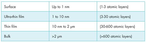
So what is a surface, and what techniques are appropriate for surface analysis? For many solid materials, we can define four regimes by depth from the outermost layer of atoms:
Thin films may often be analyzed by scanning electron microscopy (SEM) with x-ray microanalysis (EDS, WDS), x-ray fluorescence spectroscopy (XRF), laser-induced breakdown spectroscopy (LIBS), Raman spectroscopy, and many other analytical techniques. However, specialized techniques are needed in order to analyze ultra-thin and surface films. The primary surface analysis techniques for industrial samples are x-ray photoelectron spectroscopy (XPS; also known as electron spectroscopy for chemical analysis (ESCA)), Auger electron spectroscopy (AES), secondary ion mass spectrometry (SIMS), and atomic force microscopy (AFM).
XPS is a versatile technique that is very useful in measuring the surface chemistry of many solid materials. It is based upon the photoelectric effect where a low energy x-ray beam is directed at a sample in a vacuum chamber and an electron spectrometer is used to measure the photoelectrons that are produced during the ionization of sample atoms. As the photoelectrons can travel only a short distance through solid materials, only photoelectrons originating from the outermost few atomic layers of a sample can escape and be detected by the spectrometer. This is the basis for the surface sensitivity of XPS.
The photoelectrons that are analyzed provide information on the elemental composition and chemical bonding of surface atoms. For example, XPS can be used to identify and quantify surface contaminants, measure transition metal oxidation states, characterize chemical changes from plasma treatment, and compare coating thicknesses.
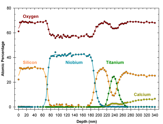
Thickness measurements and depth profiling analyses can be performed using an ion beam to etch into a sample, while sequentially analyzing the exposed surface. This produces a depth profile showing chemical concentration as a function of depth. Thin films up to a few micrometers in thickness may be analyzed with this method. For example, the figure below shows a depth profile of the multilayer coatings on a sample of architectural glass. The thicknesses of the protective silica layer on the surface, and the metal oxide, solar-control coatings, can be measured from the profile.
XPS is often used to analyze electronic components and semiconductors, polymers and plastics, metals and alloys, ceramics and catalysts, glass, and contaminants on the surfaces of materials. Designing a surface analysis investigation can be a complex undertaking, due to the need to collect samples suitable for the techniques and to preserve them from contamination. Scientists at McCrone Associates would be happy to work with you to design an investigation suitable for your application.
Comments
add comment