Scanning Electron Microscopy (SEM)
In the SEM, samples are illuminated with a focused beam of electrons in a vacuum chamber. These electrons interact with the sample in numerous ways, creating various radiation types including the production of secondary electrons, backscattered electrons and characteristic X-rays. These signals are used for imaging and compositional analysis at high spatial resolution. Compared to light microscopy, field emission SEMs (FESEMs) offer resolutions as good as 0.6 nm, greater depths of field, longer working distances and better surface sensitivity. Images of backscattered electrons (BE) provide compositional information, as the BE signal intensity of a material is proportional to its average atomic number. X-rays generated by the electron beam are detected and analyzed with an energy dispersive X-ray spectrometer (EDS). EDS spectra can be used to obtain a qualitative and quantitative elemental analysis at sub-micrometer spatial resolution.
FESEMs are typically used for varied magnifications (10-300,000× and greater, depending on the particular instrument) imaging of conductive samples. For non-conductive samples, a conductive coating of carbon, gold, chromium, etc. must be applied to avoid charging effects. Variable-pressure FESEM (low vacuum or environmental) is used for non-conductive specimens like glass, polymers, paint and biological materials without applying a conductive coating to the specimen.
Instrumentation
McCrone Associates uses several scanning electron microscopes:
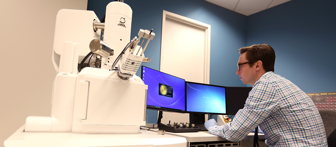
JSM-IT500HR INTOUCHSCOPE™
The high-brightness, long-life emitter delivers exceptional fidelity field emission imaging capability at any kV. The microscope also includes a large specimen chamber with variable pressure capabilities. One of the most exciting new capabilities is the Zeromag feature that incorporates digital color camera imaging with the electron column imaging to seamlessly navigate large samples. Color images of your sample automatically transition with increases in the magnification from the zero magnification color optical image to the electron imaging mode. The microscope also contains a new integrated JEOL energy dispersive X-ray spectrometer and an added Oxford Instruments energy dispersive X-ray spectrometer for exceptional analytical capability.
Resolution: 1.5 nm at 30 kV, 4.0 nm at 1 kV
Accelerating Voltage: 0.5 to 30 kV
Magnification: 0× to 600,000×
JSM-IT700HRLV INTOUCHSCOPE™
Like the JSM-IT500HR microscope, the high-brightness, long-life emitter delivers exceptional fidelity field emission imaging capability at any kV, and also includes a large specimen chamber with variable pressure capabilities as well as the Zeromag feature. The JSM-IT700HR has an innovative in-lens gun design for no wasted electrons. The microscope delivers a maximum probe current of ≥300nA. The microscope is equipped with an Oxford Instruments 150 mm2 silicon drift EDS detector and an Oxford Instruments electron backscatter diffraction (EBSD) system which can provide crystallographic information for crystalline materials.
Resolution: 1.0 nm at 30 kV, 3.0 nm at 1 kV
Accelerating Voltage: 0.5 to 30 kV
Magnification: 5× to 600,000×
JEOL JSM-7600F FESEM
Ultrahigh resolution imaging is possible with magnifications up to 1,000,000×. A wide range of operating modes and detectors are optimized for surface imaging of materials at the nanometer scale. The FESEM is equipped with an Oxford Instruments 50 mm2 silicon drift EDS detector, an Oxford Instruments wavelength dispersive X-ray spectrometer (WDS) for enhanced energy resolution, and an Oxford Instruments EBSD system. The wide range of operating modes and detectors are optimized for surface imaging and analysis of materials at the nanometer scale. The WDS system helps in instances of spectral overlaps in EDS and also permits measurement of elements to lower concentrations than EDS.
Resolution: 0.6 nm
Accelerating Voltage: 0.1 to 30 kV
Magnification: 25× to 1,000,000×
Hitachi SU7000 FESEM
The SU7000 allows efficient simultaneous acquisition of multiple signals for versatility in handling markedly different sample materials and in fulfilling wide-ranging SEM needs, from imaging a wide field of view to visualizing and analyzing nanometer-scale structures and everything in between. The specimen chamber and the vacuum system are optimized for large specimen size, sample manipulation at various axes, and variable pressure conditions. Up to six detector signals can be processed, displayed, and saved concurrently to maximize information acquisition. In addition to secondary electron and backscattered electron detectors, the microscope is equipped with a novel detector, the UVD (ultra variable-pressure detector), which functions as a secondary electron detector under low vacuum conditions, and as a cathodoluminescence (CL) detector under normal vacuum conditions. In addition, the UVD enables bright-field scanning transmission electron microscopy (STEM) detection. The SU700 is currently equipped with a dedicated STEM detector, an Oxford Instruments Ultim® Max 100 mm2 silicon drift EDS detector and an Oxford Instruments Symmetry® EBSD.
Resolution: 0.8 nm (15kV). 0.9 nm (1kV)
Accelerating Voltage: 0.1 to 30 kV
Magnification: 20× to 2,000,000×