The “Where’s Waldo” Dilemma in Microscopy
December 22, 2016
Presenter: Wayne Niemeyer, Senior Research Scientist, McCrone Associates
This webinar uses examples to show how a variety of analytical microscopy instrumentation and methodologies are utilized to conduct searches to produce “maps” revealing specific material(s) of interest. 38 minutes.
Transcript
Charles Zona (CZ): Welcome to another McCrone Group webinar. My name is Charles Zona and today our presenter is Wayne Niemeyer of McCrone Associates. Wayne is going to talk to us today about the Where’s Waldo dilemma in microscopy. Before we get started, I would like to tell you little bit about Wayne’s background and experience. Wayne is a senior research scientist with McCrone Associates and has over 35 years of experience. He specializes in X-ray microanalysis of small particles using energy and wavelength dispersive spectrometry methods with scanning electron microscopy and electron microprobe. His extensive and diverse analytical capabilities span a long career, starting in research and development for a major packaging manufacturing company prior to his employment at McCrone Associates in 1992. Wayne also teaches courses for Hooke College of Applied Sciences including Scanning Electron Microscopy and Gunshot Residue Analysis.
Wayne will field questions from the audience immediately following today’s presentation. This webinar is being recorded and will be available on the McCrone group website under the Webinars tab. Now I will hand the program over to Wayne.
Wayne Niemeyer (WN):
Thank you, Chuck and welcome, everybody. Thank you for taking time out from your schedules to join us today. I certainly hope that we can pass along some useful information for you in the meantime. I’m going to talk to you today about what I refer to as the “Where’s Waldo Dilemma in Microscopy.” I think most of you probably familiar with the Where’s Waldo puzzles, where we’re looking for our Waldo character—who is shown just below the title on the slide here—in a group of all kinds of different things. So, we’re always searching for Waldo, somehow, some way.
Here is an example of a Where’s Waldo picture. He’s somewhere in this mix of extraneous stuff, in this case a bunch of soldiers, it looks like, in different colors, and we’re trying to find where Waldo is. So, how are we doing that? We’re scanning the image. We’re scanning from left to right or up and down or in quadrants and so forth—however you would look at an image to try to find something within the image. We’re basically mapping the image in our minds.
So, for those of you that haven’t found Waldo yet, he is right there. If you still don’t believe it, there he is at higher magnification. We can see the characteristic glasses, and the hat, and red and the white striped shirt.
We’re going to do the same kind of thing: mapping for various materials in all kinds of different types of samples. I’m going to talk to you about some of the mapping and instrumentation and some of the methods that we use in microscopy. We’ll talk about the fluorescence microscope, the scanning electron microscope with energy dispersive X-ray spectrometry, the electron microprobe with wavelength dispersive X-ray spectrometry and EDS, secondary ion mass spectrometry, Raman spectroscopy, and finally, the X-ray photoelectron spectrometry method.
Let’s get started. Here’s the fluorescence microscope—one of the ones that we have in our lab; it’s an older version. It’s an Olympus BH-2 system and uses several different types of filters in the light paths and has a mercury vapor lamp (for the most part). It’s generally attached to a polarized light microscope. It’s commonly used in the reflected light mode. It uses, generally, a Mercury vapor light source—typically 100 W source, ultraviolet and violet filters are put into the light path to produce monochromatic light that impinges on our sample surface through the objective lenses. Then we view the visible wavelength light colors that come off of the sample in the eyepieces.We can observe natural fluorescence in materials which helps identify materials in many cases, or we can observe artificially-induced fluorescent dyes in materials, in other words, that have been spiked into various materials, and these dyes are known as fluorochromes.
Here is an example of a fluorescence microscopy mapping. This was a project that we worked on in conjunction with Ford Motor Company many years ago when they were having some problems with paint adhesion failure on bumpers and fascia panels of cars. They brought in some samples for us and we were able to start troubleshooting the issue, and found out in the cross sections that there was a thin film of a crystallized material right at the surface underneath what they called their adhesion promoter. In this case, that would be this blue layer up here. It wasn’t allowing this adhesion promoter solvent to penetrate through that crystallized layer into the plastic substrate, which is a thermoplastic olefin. So, we ended up having to go through a series of temperature and bake schedules that Ford Motor Company ran in conjunction with their paint supplier in order to, (not the paint supplier, but the injection molding operations) in order to minimize or eliminate that microcrystalline layer.
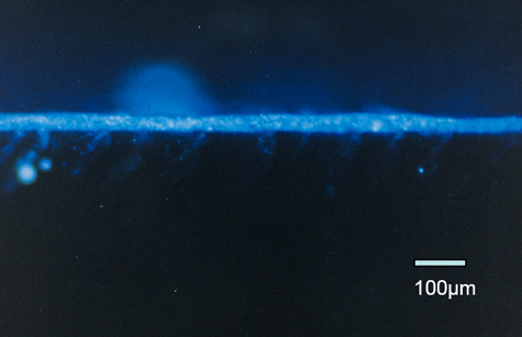
Once that was done, then they were able to put on the adhesion promoters and go through another series of experiments to optimize the bake and time schedules for the adhesion promoter to get optimum penetration under the surface, which then would allow the basecoat and the topcoat of the paint for the cars to adhere to the adhesion promoter. So, in this case, in the upper left-hand picture we have an example of no penetration. The adhesion promoter spiked with a fluorescent dye, which is fluorescing blue in the eyepieces, in this case, in the camera. There is no penetration; this would be very poor for adhesion.
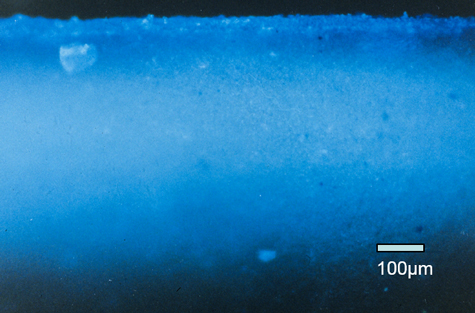
The bottom picture shows the penetration of the fluorescent dye down into the sample, in this case, approximately 450 to 500 µm penetration under the surface, which turned out to be pretty much the optimum penetration that they wanted for good adhesion on the bumpers and fascia panels.
Here’s another example from the can industry. This is a beverage can, and we’re looking at a cross-section of the top end where it attaches to the can sidewall. In this case, the beverage might be a beer or a soda that is carbonated, and it produces a lot of internal pressure inside that can. So, this seam from the aluminum end, coming around and interacting with the flange of the can sidewall, has to be a good, tight hermetic seal. To help that, there is a sealing compound that was spiked with a fluorescent dye in this case, to show the distribution of that sealing compound up through the whole seam and into this void area here to see how that has been filled in.
It’s a good way to look at the distribution of the material by spiking something with a fluorescent dye and then looking at it with a fluorescence microscope.
Moving on to the scanning electron microscope—off to the left we have our chamber where the samples are put into, it’s a vacuum system, and we have an electron beam column coming down here which produces the electron beam that will impinge onto our sample and produce all kinds of interactions with the surface of the sample. This is an X-ray detector—an energy dispersive X-ray detector—off to this side of the column. There are various monitors and so forth for the operator.
Basically, what happens when the electron beam strikes the sample and is rastered back and forth across the sample, it produces a lot of different interactions. Secondary electrons and backscattered electrons from the beam are used for imaging purposes, and X-rays are being generated from all the various elements within the sample, and each element has its own characteristic X-rays by energy or wavelength. That’s what we’re going to concentrate on today. We won’t talk any more about Auger electrons or cathodoluminescence so much.
Here is an example of how the image is formed in the SEM. The beam is rastered across the sample at a focused point to produce our image. As that beam is rastering across the sample and producing the image on our monitor, we’re also generating a lot of X-rays from every point that the beam is coming into contact with. We can use those X-rays to produce maps of a sample.
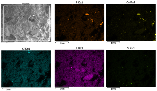
Here’s an example of a dry dog food pellet, and on the upper left we have the secondary electron image just showing the surface topography and features, and then the various maps for some of the elements that have been detected within that field of view. What was interesting here was the calcium and the phosphorus maps at the top two maps: the calcium on the right-hand side and the phosphorus in the middle. We can see that the intensities of the calcium and phosphorus are pretty much the same in several different locations. This indicates that the calcium and the phosphorus are definitely associated with one another.
We can see further down there is some silicon, some bright spots; a little bit of potassium, and some chlorine bright spots that are not associated with the calcium and the phosphorus. So, looking at the ingredient list of the dog food bag, one of the things that was on there was called fish meal. Fish meal is nothing more than ground dried fish. Here, we can see the calcium phosphorus, which is probably from the bones of the fish; bone is calcium phosphate material. So, now we can see the distribution of the crushed bone particles, their size, and so forth. This might be important information to determine how well the grind has gone, how well it’s been distributed within the pellet, and how large the particles are.
Here’s another example of X-ray and mapping imaging. This is a polished sample of a mineral showing various components in the sample. The elements that have been detected in the sample are iron, manganese, titanium, calcium, potassium, silicon, aluminum, magnesium, and oxygen, shown on the bottom here with the various colors associated with each of those elements. We can use that data to determine what types of minerals are actually present in this field of view.
The first one is ilmenite, which the arrows are pointing to—kind of the aqua-blue coloration areas here, and there is another one over here. Ilmenite is an iron titanium oxide, and so the colors are from the color of the iron and the titanium—kind of a greenish color, and the oxygen—a little deeper green, so that’s what is producing this color here.
Then we can have biotite, which is this whole big region—almost a matrix region, here. That’s a complex mineral of the mica family and is mainly potassium, magnesium, aluminum, iron silicates, and varying ratios of those elements, and so forth. Again, most of these elements are present so we get kind of an oddball-looking color here. Then we can go on and pick up quartz, which is the greenish yellow material; that is silicon dioxide, and the yellow silicon and the oxygen green is producing this greenish-yellow, colorful quartz: silicon dioxide.
Garnet is another complex mineral. It’s the garnet group of minerals, actually, and is calcium, iron, magnesium, manganese, chromium, aluminum, and so forth. Those kinds of elements could be present in many different ratios for that garnet family of minerals. Then we have orthoclase, which is a potassium aluminum silicate mineral; and then we have anorthite, which is a calcium aluminum silicate mineral. So, we can see how we can use these mapping techniques to identify the mineral phases within this kind of a sample.
Moving on to the electron microprobe, this one is known as the Superprobe— the JEOL JXA-8200 Superprobe; I call this an SEM on steroids. We have the same sample-type chamber and the electron beam column; here’s our X-ray detector, the EDS detector; and what makes this a microprobe is the wavelength spectrometers that are around the column. In this case, there are five spectrometers on the column. Each spectrometer of wavelength can analyze only one element at a time, whereas the EDS X-ray system can analyze all of the elements of the periodic table from boron through uranium all at once. That’s why a lot of people really prefer to use energy dispersive X-ray analysis for most of their work. Wavelength analysis is really good for trace evidence analysis, trace elements analysis, and for good, solid quantitative analysis using known standards for each element that’s being detected.
But anyway, on the mapping part of it, here’s an example of a meteorite cross-section that’s been polished. It’s from Northwest Africa—that’s the NWA designation. These are several of the maps that we found. There are all kinds of elements; I think there are about 15 of them altogether. Here are examples of magnesium, silicon, and oxygen, which would be magnesium silicate type of minerals. We can see on the right-hand side of each image there’s a color scale bar, which is an intensity bar. The blue colors are lower intensity of that element, and the red and pinks are higher intensities of each of those elements. We can see those different intensity levels within the various grains on the map.
It’s a large area map; the electron microprobe allows us to move the stage underneath the beam—keep the beam stationary and move the stage back and forth under the beam—to produce large area maps. In this case, this meteorite was about 2.5” x 3.5” in size.
Here’s another example of the meteorite looking at a higher magnification view near the center of that cross-section. Now we’re looking at a backscattered electron image and again, this is kind of a mapping technique as well, because we’re seeing brightness and contrast differences due to average atomic number of the material. These darker areas, the dark gray areas, are low atomic number materials, and then we have kind of medium gray areas, in here and down at the bottom, that are moderate atomic number materials, and then the lighter materials are higher atomic things, higher atomic number things.
Here’s what a wavelength dispersive X-ray map would look like on that same image, and now we can clearly see the distribution of these elements and their association with one another. For example, nickel and phosphorus on the right-hand side are obviously—there’s a big section right in the center that’s obviously associated with higher quantities of nickel and phosphorus. These are nickel phosphides and commonly found in meteorites. On the left-hand side we see some association of sulfur with the iron. In this case, this region here is kind of yellowish and then the bluish region of iron up on the top in the same area, and a couple of the others in the same area; this little forked-prong one is iron and sulfur. These are iron sulfides and are also very commonly found in meteorites. Again, we get a good idea of the distribution of the various elements and their associations.
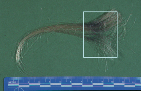
Here is an example of gunshot residue. I sometimes can’t resist doing something with forensics. I do a lot of gunshot residue analysis here, and everybody likes forensics, especially now with the CSI programs on TV. This is a case where a woman was claiming that her domestic abuse husband had shot a gun right near her head during an argument and ran from the house, ditched the gun, and was captured later by the police. While the police were interviewing her, they noticed that there was a dark smudge in her hair, and what they did was they collected a lock of that hair with the smudge and sent it to us, and asked if we could determine if this black area in here on her hair was filled with gunshot residue particles or if it was just ordinary dirt.
Gunshot residue particles are produced from a gun, when it’s fired, from the primer components of the cartridge at the back cap of the cartridge that’s struck by the firing pin. Those compounds that are in there contain lead, barium, and antimony, and when they vaporize, they recondense in any combinations of lead, barium, and antimony. But if particles are found that contain all three of those elements, they are considered as characteristic of a gunshot, and they’re typically sub 10 µm in size, so we have to use the scanning electron microscope to look for them.
Here’s what the hair looked like in transmitted light microscopy. On the left, we have one strand from the dirty hair area, and on the right-hand side, just some examples of what clean hair would look like in the transmitted microscope. We can see on the left-hand side the dirty hair is definitely covered with a lot of material that really darkens it. What we did is we took that strand of hair and put it onto a piece of tape, and basically dabbed it on a couple of times onto that tape—so we’re virtually lifting the particles off of the hair strand and putting them onto the tape, and then we can analyze the tape.
Here on the upper left is a backscattered electron image on the scanning electron microscope showing the bright areas all over the place, and high atomic number—very bright compared to the tape background which is mostly just carbonaceous organic material, the adhesive. On the right hand side we have the SEM image of the particles at higher magnification, and then the three corresponding maps that go with that image. We have the lead on the right top, the barium on the left bottom, and the antimony on the right bottom. We can see by looking at these maps that the lead, the barium, and the antimony are all associated with one another in these various particles, especially the larger ones—definitely gunshot residue. It certainly corroborated her story that he fired that gun right near her head.
Moving on to secondary ion mass spectrometry, many of you may not be familiar with this type of instrumentation or technique. This is the system that we have; it’s a Cameca IMS 1280. As you can see, it’s quite large; it takes up a good part of a big room. The ion source for the beam and the specimen chamber are over here on the left-hand side behind the monitors, then back behind the monitors, this long tubular feature—that’s our mass analyzer, and then we have a powerful magnet system that end up sending the ions that are sputtered off the surface to our detector to produce a spectrum of atomic mass versus counts. This unit can detect every element of the periodic table: hydrogen through uranium on up. So it’s very, very good if we’re going to be looking for something like lithium in a suspected lithium grease, for example. Lithium is not easily detected at all by wavelength dispersive X-ray spectrometry or by energy dispersive X-ray spectrometry. The units for that are not very sensitive to lithium or boron, or beryllium, so the SIMS system is very sensitive to most of the elements down to the parts per million or even parts per billion range.
Here’s how the SIMS process works.It’s a sputtering process, so it is somewhat surface destructive on a molecular scale. The primary ion beam comes down and strikes the surface of the sample producing all kinds of ionizations, which are secondary ions, there are various atoms and atom combinations sent out, electrons, photons, and all kinds of things. The primary ion source then strikes the sample. A lot of the secondary ions are ejected from the surface of the sample and go through the mass analyzer, and finally are separated out by their atomic mass into the detector system to produce our spectrum. Primary ion beam can be oxygen, it can be argon, cesium, gallium—we typically use oxygen and argon; once in a while we might use cesium if we need to do more of a depth profile to sputter away much more the surface—get down into several micrometers of depth. We can also focus on any atomic mass and map it.
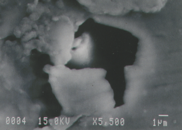
Here are some examples. Here’s a coating crater in an aluminum can—the inside of the aluminum beverage can, which is coated with a clear coating material. In this particular case, the coating was interacting with something on the surface of the metal that caused it to pull back into this circular area, called a crater.
Right in the center, as we look at higher magnification in the scanning electron microscope, we can see down at the bottom left that this is a corrosion pit. It is a very, very aggressive corrosion reaction that has gone on here to produce this pit in the sidewall of the can before the coating was even applied.
So, here are the SIMS maps. We had done all kinds of the analyses within these pits with SEM EDS, we did extractions for organic analysis for FTIR, and so forth, and came up pretty empty. So, we resorted the SIMS and we did some SIMS mapping, and we found—lo and behold—here we have calcium, boron in the middle, and iron at the bottom of the maps, all associated with one another, all three elements associated with one another. We have the color scale bars on the left showing yellow, higher concentrations, and down into the reds and purples are lower concentrations. We can see that these are the darker colors around the perimeters of the particles and then higher concentrations in the center. These are not flat particles; these particles are varying in thickness.
Some more examples: here’s the same pit again, here’s another one showing the same correlation of calcium, boron, and iron. What was crucial here was the presence of the boron. Boron is very difficult to detect by these other methods, as I mentioned earlier, but by SIMS it’s quite easily detectable. This was a key clue as to what was causing the problem. Boron or borate salts are used as corrosion inhibitors in cooling water towers. The cooling water tower is used in the in the production plant here to keep a lubricant system, that’s a 7,000 gallon system, cooled down while the manufacturing process is going on to make the cans. It’s a very intensive drawing and ironing operation of the aluminum which produces a lot of friction heat, and that heats up that lubricant system considerably. The cooling tower water circulates around that big tank to keep the coolant down to a lower temperature of around 100° or so Fahrenheit.
The borate was a big key here because that indicated to us, along with the calcium and the iron, that we might have a cooling tower water leak in our lubricant system. Low and behold, when they dumped the system and inspected the heat exchange tubing and what-not, they did find fairly large crack in one of them, and that’s what the stuff was leaking into our coolant.
The cooling tower water was also maintained at a fairly high pH, up around nine or 10, and anything around that high of a pH is going to severely corrode aluminum. The borate salt is not a corrosion inhibitor for aluminum, it’s only used for the iron and steel in the cooling tower. This is what led us to the cooling tower water leak into the coolant system. Once they fixed that and refilled the system again with new coolant, they were off and running, and their problem was solved.
Here’s another example of SIMS ion images. Here, we were looking at a field of particles, looking for something that contained beryllium. Beryllium is very sensitive for detection limits in SIMS compared to the other techniques that we‘ve talked about. Here we can see that there is quite a distribution of various particles that are high beryllium content materials.
Moving on to Raman spectroscopy, this is the Raman InVia microscope. It’s equipped with three lasers, so we have three different wavelengths of laser light that we can use to push through the microscope and down onto our sample through the objective lens. We can use it for mapping all kinds of different things, for example, pharmaceutical tablets—maybe some distribution of active ingredients; art conservation; forgeries. We can map inks and pigments, electronics, rocks of course—distribution of minerals similar to what we did with the EDS mapping, and more, of course.
Spatial resolution is several millimeters down to about a micrometer in this system. So, what we’re doing here with the Raman spectroscopy, our laser light is our incident light coming onto the sample, and what happens then is that light is then scattered in two different ways. One is just the scattered light, the Rayleigh scattering as they call it, where the wavelength really is not changing. But there’s other inelastic scattering by Raman where the light coming back to the detector is a slightly different wavelength than the laser light wavelength. That difference in wavelength is an indicator that corresponds to a vibrational mode in the molecular structure of the crystalline material, very similar to the infrared spectroscopy. In fact, both infrared and Raman spectroscopy are considered as complementary techniques. Some things that can’t be easily detected in the infrared can be easily detected by Raman, and vice-versa. This gives us information about molecular groups and crystalline structures.
Here’s an example of the Raman mapping where we can focus in on specific components that are unique to a compound. In this example, we’re using the compound of calcium carbonate looking at one Raman peak that’s unique to calcium carbonate, and also now one Raman peak that’s unique to sucrose. We can map that within this area where the light microscope image is; this is the distribution on a filter media, and we can also overlay the maps onto each other looking at distribution of materials; we can look at particle size of the materials, same kind of thing.
Moving on now to the XPS, or ESCA, microprobe, this is the Physical Electronics Quantum 2000 and it’s not much to see; it’s just a big gray-tan box, basically. If you want to call it a black box, fine. Here’s our sample chamber introduction port and it goes into a sample chamber that’s under ultrahigh vacuum, on the order of 10-10 to the 10-11 torr, so it is very high vacuum. It is actually used for very, very sensitive surface analysis to identify not only the elements, but also some possible compound information from those elements within a couple hundred angstroms of the surface. It doesn’t penetrate nearly as deeply as the SIMS unit does or the scanning electron microscopes and microprobes, or even the Raman. It’s a true surface analysis piece of instrumentation.
Here’s how it works: inside there is an electron gun similar to the electron guns that would be in the scanning electron microscopes. The electron beam is impinged onto an aluminum anode. The X-rays from the aluminum are then collected in an ellipsoidal monchromator and focused down onto the sample. So, it’s X-rays that are used for the beam instead of electrons or oxygen plasmas and so forth. These photo electrons that are produced from the sample then are collected through hemispherical analyzer into a multichannel detector, and then finally produces a spectrum for us, which gives us the elemental composition, but also the spectrum is binding energy versus counts. The binding energy is important to specific compound information. I’ll show you that in just a minute.
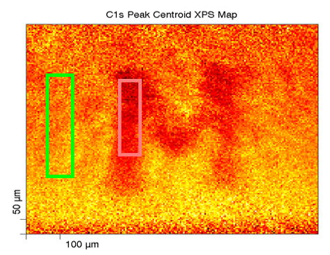
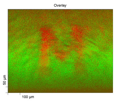
Here we have XPS chemical state mapping where we are looking at, in this linear least-squares fit basis spectra on the upper right, looking at a paper with a toner ink on it. We can see on the carbon—this is the carbon band (the carbon 1s band) and its binding energy—the paper has the binding energy right around 284.8, something like that; whereas the toner ink, another carbonaceous organic material, has a binding energy down around 284 eV, so they’re separated. We can focus, for mapping purposes, on the binding energy for each of these two compounds and produce the maps that are shown here.
On the lower right, we have the green map which is representative of the paper carbon peak, and then the red map to the right of it is the toner map for the carbon, and then we can overlay them together and we can see the distribution of these two carbonaceous compounds—something that you would probably not be able to do by most any other methods other than maybe infrared spectroscopy if you had specific peaks that you could look at; absorbance bands.
In summary, the “Where’s Waldo” dilemma in Microscopy can be solved as far as I’m concerned, anyway. There’s multiple instrumentation and methods that can be employed to produce the distribution maps of materials, so you can look at their association with one another, their particle sizes, and so forth. If it’s there, we’ll find it. As you can see, there’s a lot of instrumentation available for different types of materials. Okay, I know, “if it’s there, we will find it,” that’s a strong term. I’ll give this to you, okay, most of the time we’ll find it.
The choice of the instrumentation and method is sample dependent. This is where it’s really crucial; it requires very careful strategic planning with the client to provide the most useful results, the most beneficial results, to the client.
So, I thank you for taking time out to join us today, and I guess I’ll be available now to take some questions.
CZ: Thanks, Wayne. Thanks again everyone for attending today’s webinar. If you have any questions please go ahead and type them into the question field, and Wayne will start to answer them as they come in.
WN: You can also email me. My e-mail address is shown there at the last slide so if you have something that you want to discuss in more detail, either e-mail me or tell me to give you a phone call, whatever you’d like.
CZ: While we are waiting, Wayne, I’ll ask you a question. Do you have a go-to instrument, let’s say, where you start out most of the time looking for Waldo, in this case?
WN: It really is sample-dependent. Certain things aren’t very compatible with electron beams for the scanning electron microscope and microprobe. They might be nonconductive materials, in which case it’s very difficult to do some mapping because we have to spend a lot of time on specific areas with electron beams, and that can produce all kinds of thermal damage and artifacts. It’s just a matter of what the sample is and what the client really needs from it. I would say the SEM EDS mapping is probably the most used, around here, anyway, but XPS mapping is also very handy. Raman mapping is something that we haven’t done a whole lot of, but as we do more, we’re discovering that it’s extremely beneficial, and sometimes the only way we get the maps that we need.
CZ: It looks like we have a question here from Margaret. She wants to know, “When is Raman versus infrared more appropriate?”
WN: Raman spectroscopy was mainly developed for identifying minerals, mineral phases, oxides and things like that, and silicates, phosphates, carbonates, and stuff like that. Where infrared spectroscopy is mainly used for identifying organic materials, but they can also be used in conjunction with one another as complementary techniques, as I mentioned earlier. If you have the right type of detectors on the infrared system you can analyze minerals, as well. With Raman spectroscopy you can also identify organic compounds. It just depends on how the molecular structure and crystalline structure is set up. As I said before, they’re really complementary techniques. There are certain things that don’t work well in infrared spectroscopy, but work very well by Raman, and vice versa. So, you really don’t know for sure. If you have both systems available, you try one first, depending on what type of sample it is and what information you know about the sample, and then if it doesn’t work we’ll go ahead try the other one. If one won’t work, the other one might.
CZ: We have a question from Jan: “Have you ever considered NIR imaging? Currently, we use it for foreign particles on tablets.”
WN: Near-infrared imaging is quite useful for that, and is it’s very sensitive and it’s certainly good. We do not have it here, but it’s certainly another technique that can be used. The other question was clarifying the NIR mapping, that it’s much faster distribution than some of the other techniques. Yes, it definitely is.
CZ: I think that will about do it on the questions, Wayne. Thanks again everybody for your of attendance and interest, and be sure to join us for our next webinar on December 19 when our presenters will be Jim Bristol of McCrone Microscopes and Accessories, and Adam Babarik of Midwest Information Systems. Jim and Adam will be discussing stringent 21 CFR part 11 compliance issues related to digital imaging, and PAX-it software’s recent advances related to those issues. We hope to see you then.
Comments
add comment